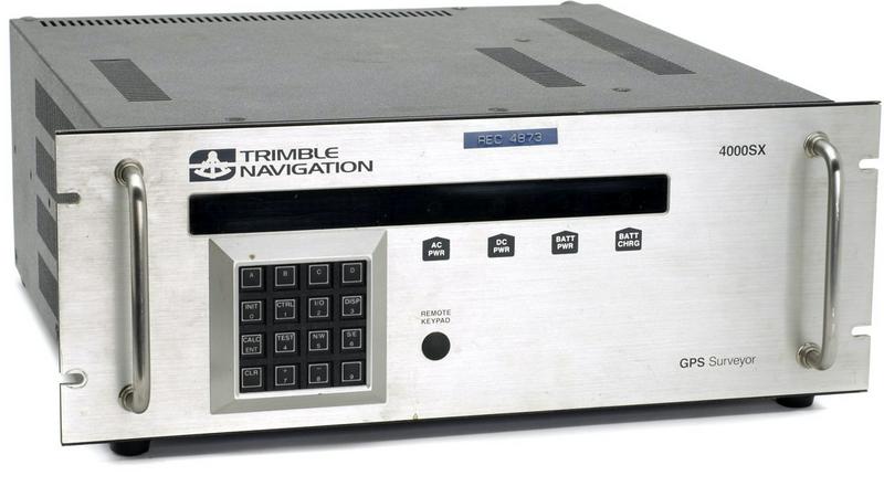
Trimble 4000SX Deep Dive
ROM Images
| ROM | Label | Board Marks | File |
|---|---|---|---|
| U36 | U-36 Rev 3.30 4000 Chk Sum 52EA | ROM0-U | U36.rom |
| U37 | U-37 Rev 3.30 4000 Chk Sum 2500 | ROM9-U | U37.rom |
| U38 | U-38 Rev 3.30 4000 Chk Sum E240 | ROMA-U | U38.rom |
| U44 | U-44 Rev 3.30 4000 Chk Sum D16B | ROM0-L | U44.rom |
| U45 | U-45 Rev 3.30 4000 Chk Sum 8E92 | ROM9-L | U45.rom |
| U46 | U-46 Rev 3.30 4000 Chk Sum 0717 | ROMA-L | U46.rom |
Merged ROM Images
| Bank | File |
|---|---|
| ROM0 (U36+U44) | ROM0.bin |
| ROM9 (U37+U45) | ROM9.bin |
| ROMA (U38+U46) | ROMA.bin |
Memory Map
000000 - 003FFF ROM0
004000 - 007FFF RAM
090000 - 09FFFF ROM9
0A0000 - 0AFFFF ROMA
Flight Case Cannon Connector Pinouts
| Purpose | Connector | Pinout |
|---|---|---|
| AC Line In | Cannon MS3106A14S-7S |
A Line B Neutral C Ground |
| DC Power | Cannon MS3106A10SL-4S |
A Positive B Negative |
| RS232C | Cannon MS3106A14S-5S |
A Signal Ground B Transmit Data C Receive Data D CTS E DTR |
Firmware Teardown
Unlike later receiver models like the 4000ST, The majority of the firmware running on the 4000SX runs inside a stack based virtual machine. I have reverse engineered most of the Instruction set. I have also created a disassembler for the virtual machine code contained in the ROMS.
Disassembly at my current level of knowledge: disassembly.txt
PCB Photos
10670 - DAC
Component side

Copper side

10850 - Synthesizer
- J20 - 768F0 IN
- J21 - 38.4F0 OUT
- J22 - 16F0 OUT
- J23 - 768F0 TUNE OUT
- J24 - 16F0 TUNE IN
- J25 - LMTR OUT
- J26 - LMTR IN
Notes
- J21 38.4F0 OUT is derived from 768F0IN (768/4/5=38.4)
- J22 16F0 OUT is derived from a local oscillator. The Lock board compares this signal to the OCXO, and produces a tune voltage to tune the frequency of the local oscillator.
- J25 LIMITER OUT is derived from J25 LIMITER IN, and is completely separate from the synthesizer functionality.
On the board shown, Tantalum capacitor C24 had shorted, as they do, which shorted the output of regulator U10. This caused L7 and L8, the two inductors in series on the input of U10, to overheat, which is why the board is discoloured in that vicinity. This failure eventually burned out the 1.5A fuse in the power supply protecting the +14V rail. The charred inductors were replaced, as were all tantalum capacitors.
Component side

Copper side

10853 - Mixer/VFO
- J30 - 768F0 OUT
- J31 - 768F0 TUNE IN
- J32 - ?
- J33 - LMTR OUT
- J34 - ANT IN
Component side

Copper side

10924 - Lock Board
- J40 - 16F0 TUNE OUT
- J41 - FREQ OUT
- J42 - FREQ IN
- J43 - 16F0 OUT
- J44 - 16FO IN
Component side

Copper side

Other Stuff
The OCXO is a Piezo Systems 2810007-23, which is a clone of the HP 10811B.
Mixer/Lock/Synthesizer Module Power Cable
The Mixer (10853), Lock (10924) and Synthesizer modules (10850) are interconnected with a 10 conductor ribbon cable that is used to distribute power among the cards. Pin 1 is closest to the aluminum faceplate of the card, and closest to the J20/J30/J40 end of the card. The pinout:
1  +12V for OCXO (Produced from +14V by U31, an LM317 on lock board)
2  GND for OCXO
3  -12V (Produced from -14V by U11, an LM337 on synthesizer board)
4  GND
5  -14V (provided by system power supply)
6  +12V (Produced from +14V by U10, an LM317 on synthesizer board)
7  GND  (probably)
8  +14V (provided by system power supply)
9  +5V  (provided by system power supply)
10 +5V  (provided by system power supply)